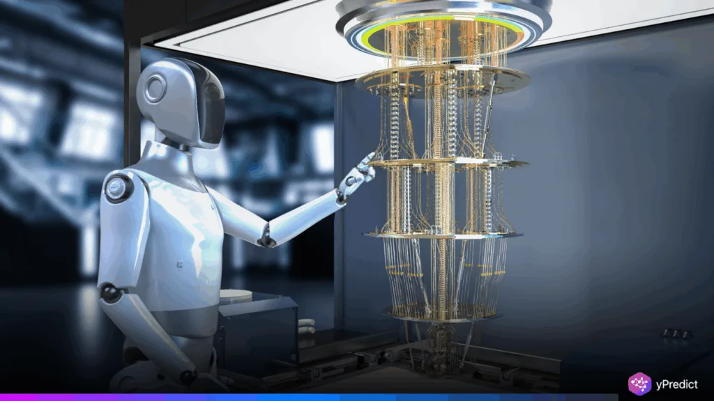
There is also recent work that indicates that physics-based Application-Specific Integrated Circuits (ASICs) may be able to transform AI hardware based on utilizing natural processes such as memristors and stochastic junctions. Neuromorphic-based chips could cut energy consumption by up to 90 percent over older silicon designs. It has been termed a trend that reflects longer anticipated diversification in architecture and is consistent with increased interest in the energy consumption of AI training and inference. Such systems, though prospective, have practical fabrication and scale-up problems, particularly in incorporating novel materials. Nevertheless, their future capabilities to solve the heat, latency, and energy bottlenecks put them on the edge of ever-evolving hardware in AI, especially edge and scientific computing.
Leveraging Physical Phenomena for AI Hardware Efficiency
In physics-based ASICs, hardware performs computation using physical phenomena, including electrical resistance in memristors or magnetic dynamics in tunnel junctions. A 2023 Nature Communications research demonstrated energy efficiency gains of up to 90 percent in memristor-based circuits, including binarized neural networks. Simulating biological synapses, the devices are extremely good at evaluating weighted summations without separate memory-fetch instructions and thus overcome the von Neumann bottleneck. The property is particularly valuable to neuromorphic computing and edge AI implementations, where the energy used is more important than the raw throughput. The devices operate by analog or stochastic signals in contrast to traditional digital chips, and they allow continuous-state computation.
Their ability to save on energy is because of the lesser data flow and smaller data set storage, and this makes them a perfect fit in the low-power requirements of sensors and mobile AI, and environmental monitoring applications. And besides, stochastic or resistive physical network-based systems are naturally parallel and can hence be used on AI loads such as convolution and attention mechanisms. Such inventions are non-theoretical; trial prototypes already attain orders-of-magnitude increases in operations per watt. Nevertheless, with these discoveries, scaling and batch-to-batch consistency have been cited as being major roadblocks to commercialization. The capability to compute using matter itself is, however, coming up as a new core concept in redesigning efficient AI calculation of the decade to come.
Hardware Diversification and Strategic Industry Implications
The transition to physics-based ASICs reflects general trends of changing approaches to AI hardware. The end of Moore’s Law and Dennard Scaling has led to a widespread effect of a possible lifelessness of Moore’s Law, an effect known as a carefulness explosion (Cambrian explosion) of computing proposals, as per John Hennessy and David Patterson in the 2019 Turing Lecture. Rather than building on general-purpose chips such as GPUs, developers are tailoring domain-specific architectures to better execute particular AI tasks, which include transformer inference, along with low-latency edge applications. This change in architecture also depicts actual issues of scalability, yield, and thermal control of the current AI infrastructure.
As large language models grow, energy demands have ballooned, prompting interest in hardware that reduces operating costs and environmental impact. Physics-based approaches could serve as an alternative or complement to dominant players like NVIDIA, especially in contexts where GPU-based scaling is no longer tenable due to power or supply-chain constraints. Moreover, interest from national labs and defense sectors suggests potential crossover into scientific computing and on-chip intelligence for high-energy physics experiments. As AI becomes increasingly embedded in physical environments, from satellites to autonomous labs, hardware that “thinks” like the systems it monitors could become not just efficient but necessary.
Fabrication Challenges and the Path to Practical Deployment
Despite their promise, physics-based ASICs face significant fabrication hurdles. Integrating novel materials like memristive oxides or magnetic layers into silicon workflows is difficult, as is ensuring uniformity across chips. A 2024 IEEE Transactions on Electron Devices report underscores reliability, process variability, and interface control as key limitations. These issues restrict commercial scalability and require new design methodologies and tools for verification. However, continued investment in co-design strategies, where models and hardware evolve together, may unlock their potential. If solved, these challenges could usher in a new era of energy-efficient AI hardware. Will the next AI leap be powered not by silicon, but by physics itself?


