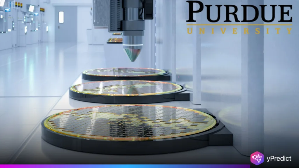
Purdue University’s AI-Driven X-ray Imaging Revolutionises Semiconductor Quality Control
Purdue University is at the forefront of a transformative advancement in semiconductor manufacturing, leveraging artificial intelligence (AI) and high-resolution X-ray imaging to detect minuscule defects in chips. These defects, often smaller than a human hair, can lead to significant malfunctions in critical systems such as automotive steering mechanisms and consumer electronics like smartphones and laptops. By integrating AI with X-ray imaging, Purdue aims to enhance the reliability and efficiency of semiconductor production.
AI-Powered X-ray Imaging: A Breakthrough in Defect Detection
The collaboration between Purdue University and Argonne National Laboratory has led to the development of a cutting-edge approach that combines X-ray imaging with AI to identify tiny defects in semiconductor chips without causing any damage. This innovative method utilises high-resolution X-ray tomography to create detailed 3D microstructures of packaged devices, enabling researchers to trace defects back to their origin in the manufacturing process. AI algorithms then analyse these images to automate defect detection, significantly accelerating the inspection process and improving yield.
Enhancing Manufacturing Efficiency and Reliability
Traditional methods of defect detection often involve destructive cross-sectioning, which can be time-consuming and wasteful. Purdue’s AI-driven X-ray imaging offers a non-destructive alternative, allowing for periodic in-process imaging that preserves the integrity of the components. This approach not only shortens failure analysis cycles but also enables higher throughput analytics, reducing operator time and facilitating scalable, line-ready inspection. By linking defect classes to field reliability, manufacturers can set tighter, evidence-based screening criteria, leading to higher yield without unnecessary scrap.
Addressing the Challenges of Miniaturisation in Semiconductor Packaging
As semiconductor packaging becomes increasingly complex, the risk of defects that escape traditional inspection methods grows. Purdue’s research focuses on identifying where and how defects arise during packaging and which assembly steps are most susceptible. This comprehensive analysis creates a map of risk across the process flow. It guides targeted interventions instead of blanket slowdowns or rework. By automating defect detection and prioritisation, Purdue’s approach helps manufacturing teams focus on the most critical issues. This, in turn, enhances overall production efficiency.
Conclusion: Paving the Way for Future-Ready Semiconductor Manufacturing
Purdue University’s integration of AI with X-ray imaging represents a significant leap forward in semiconductor quality control. This innovative approach enables faster, non-destructive detection of microscopic defects. It improves the reliability of semiconductor components. It also enhances the efficiency of the manufacturing process. As demand for smaller, more powerful chips grows, Purdue’s advancements are setting new industry standards. They ensure the next generation of electronic devices meets the highest quality and performance benchmarks.